Research Unit for Aerospace Materials Evaluation Technology
KEYWORD
- Measurement Technology development
- MEMS Sensor
- Piezo electric device
- Dielectric materials
- Spacecraft and aircraft materials
Development and implementation of MEMS pressure wave sensor with submicron ultra-high position resolution
Aim: Achievement of charge measurement with sub-micron position resolution using thin-film pressure wave sensor with ps-ns time resolution developed by MEMS technology for pulsed electroacoustic method.
- ●Adapting the developed sensors to electric aircraft and charging sensors for lunar exploration ⇒Promoted as flagship research
- ●Building a platform for a basic aerospace technology development by promoting this research in collaboration with external organizations
Research staff
Professor・Department of Mechanical Systems Engineering

Professor・Department of Mechanical Systems Engineering

Professor・Department of Electrical, Electronics and Communication Engineering

Associate Professor・Department of Electrical, Electronics and Communication Engineering

Role and purpose of the laboratory
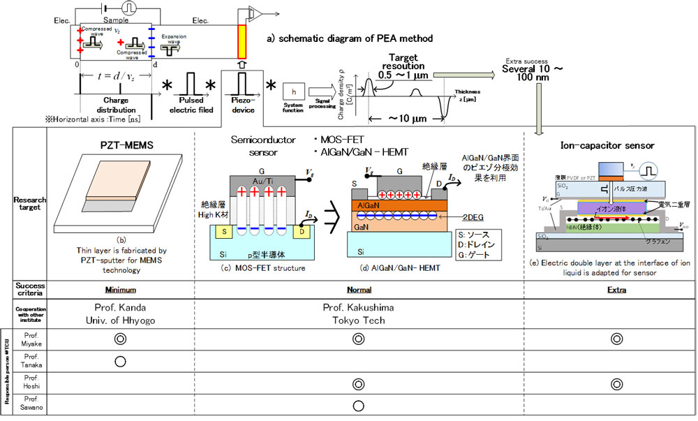
Recently, the space charge distribution of insulators with sub-µm to several dozen nm positional resolution has been desired for motor windings, photoconductive films, and electronic components etc. In addition, there are cases of severe environmental conditions such as high temperature and radiation. In order to meet this demand, we will develop a piezoelectric PZT thin film using MEMS technology and a semiconductor sensor using a depletion layer as the polarization structure of a piezoelectric element to improve the positional resolution up to submicron in the pulsed electroacoustic (PEA) method. This method can obtain the charge distribution from the intensity and propagation time of nanosecond pulsed pressure waves generated from the accumulated charge.
The developed sensor will be applied as a sensor for the PEA method, aiming to realize the charging measurement of thin films.
Research Projects
- ● Development of high-resolution pressure wave sensor using thin-film piezoelectric element based on MEMS-PZT
- ● Development of super high resolution pressure wave sensor using AlGaN/GaN heterostructure HEMT
- ● Development of extra super high resolution pressure wave sensor using ionic liquid electric double layer capacitor + MEMS-FET sensor
- ● Implementation of the developed sensor into the PEA method to measure the space charge distribution in a thin film insulator with a thickness of less than 50 µm.
Characteristics of research and development technologies
- ● PZT has good piezoelectricity, but it was very difficult to make thin films. However, thanks to improvements in sputtering technology, it has become possible to create films with a thickness of less than 3 µm, enabling us to do this research.
- ● We will apply a pressure wave sensor based on MOS-FET structure with AlGaN/GaN heterostructure HEMT, which is expected to be used as a high-speed, high-power, and high-efficiency device for various green ICT technologies.
- ● The ionic liquid electric double layer capacitor + MEMS-FET sensor uses the electric double layer formed at the interface between the ionic liquid and the electrode. This sensor aims to measure the charging in the micro region of nm order, which is beyond the conventional concept for pressure wave sensors.