Research Center for Nano-Electronics
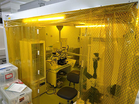
Clean room
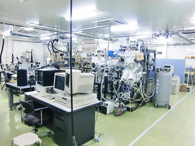
Semi-clean room
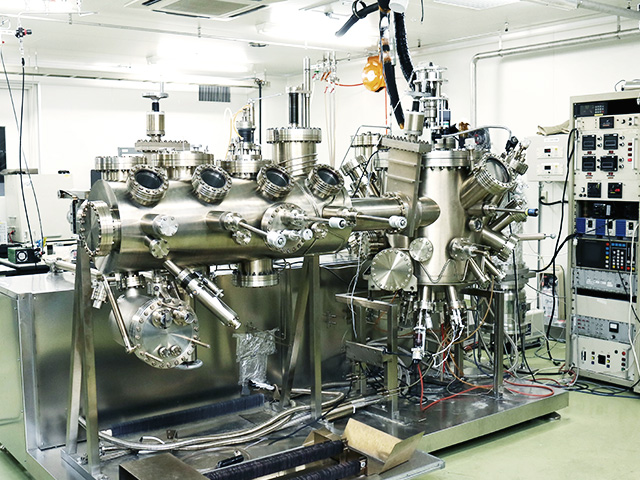
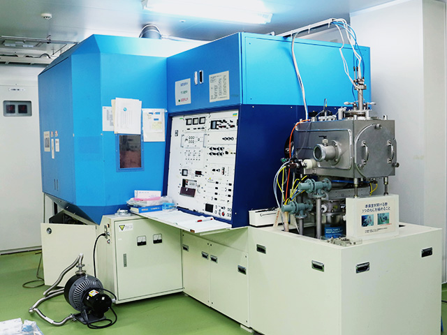
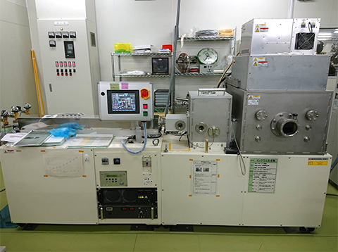
Silicon molecular beam epitaxy (MBE)
This device is used for crystal growth of new Si-based nanometer-scale semiconductor materials.
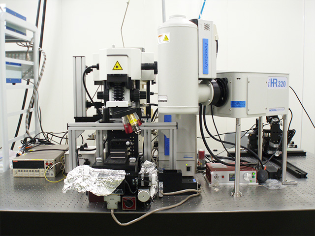
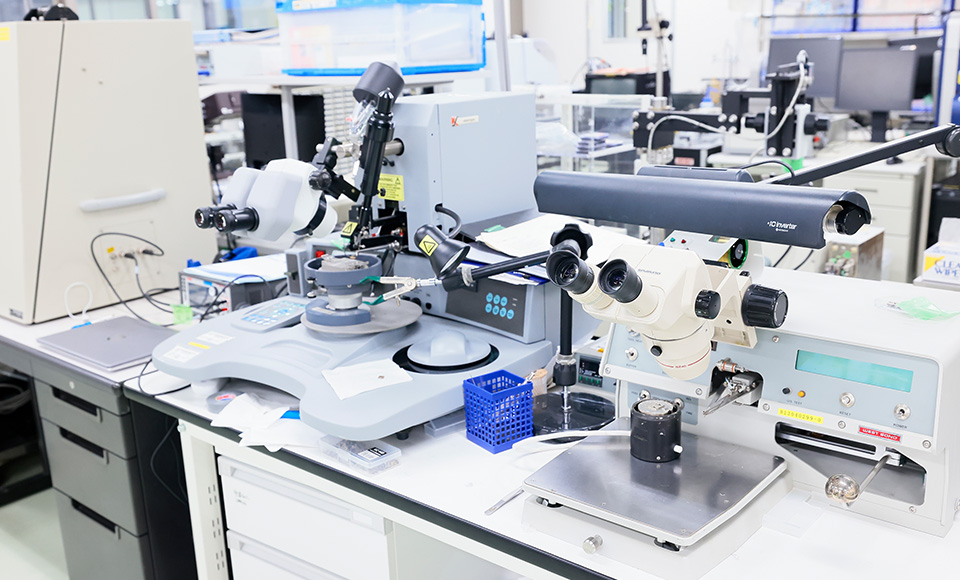
Micro-PL spectrometer
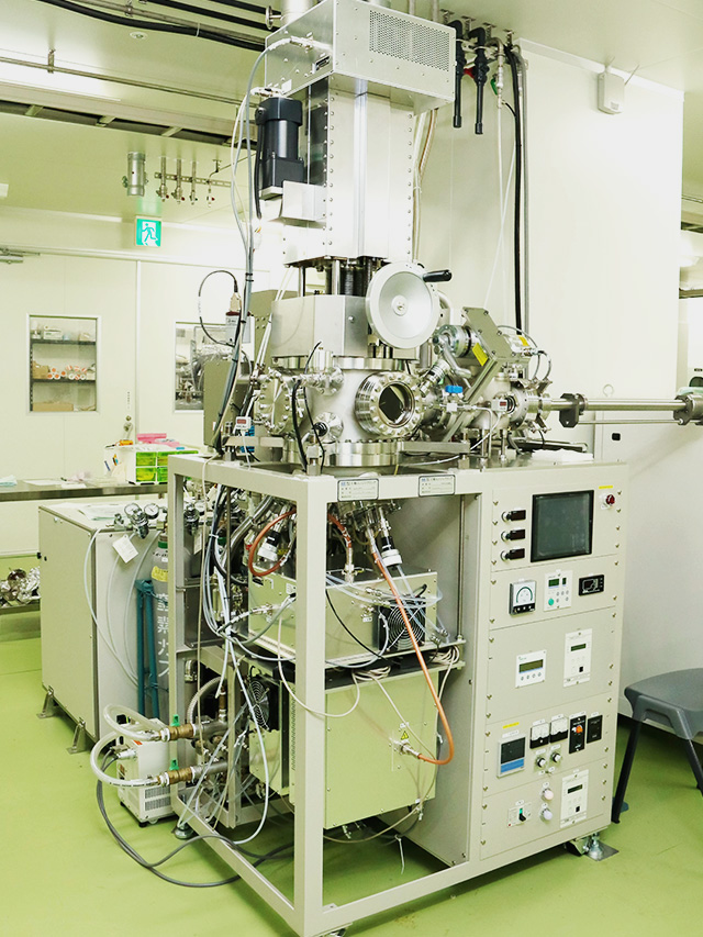
Ion implanter
For doping of semiconductor by ion impurities
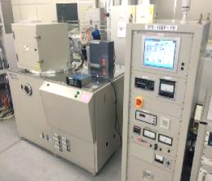
Electron beam lithography
This device is used for the patterning of nanometer-scale semiconductors.
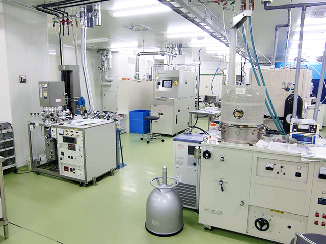
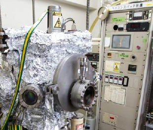
Sputtering
Research Center for High Efficiency Hydrogen Engine and Engine Tribology
(1) Friction force evaluation system for multi-cylinder engines
(2) Friction force measurement system based on floating liner method
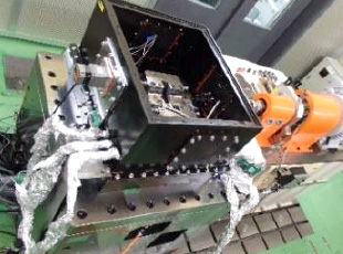
(3) Friction force measurement and seizure evaluation unit system for plain bearings
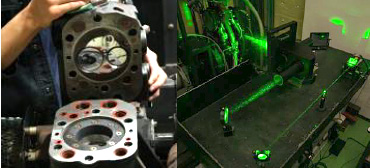
(4) Optical Hydrogen Engine to Visualize Hydrogen Jet and Flame Propagation
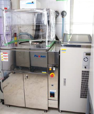
(5) Atomic layer deposition (ALD) system for fabricating nano-order thin insulation layers on thin-film sensors
(6) Sputtering Equipment to Fabricate Thin Film Sensors for Measuring oil film condition in Engine Sliding Surface
(7) Sputtering Equipment to Fabricate Thin Film Heat Flux Sensor
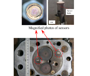
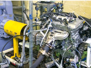
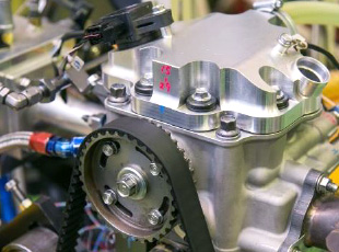
(8) Heat Flux Sensor Installed on Hydrogen Engine Combustion Chamber
Research Center for Geotechnical & Geo-environmental Studies
Centrifuge apparatus
This specialized experimental apparatus enables us to simulate actual sized models by testing miniaturized models at high rotational speeds. Although such experiments are still rare elsewhere, we have more than 20 years of experience in this field.
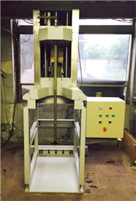
Model ground improvement machine
This machine is used to produce improved pile-formed body borings by using special screws that mix the ground and cement. In this center, we investigate the most effective screw shapes and the best soil/cement ratios by considering temperature and soil property influences.
Intelligent Robotics Center
Testbed for developing mobile robots
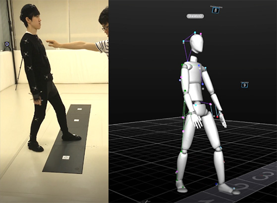
We use force plates to estimate both floor reaction force and joint torque.
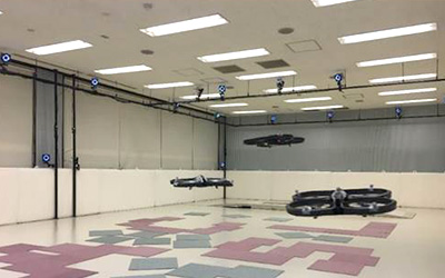
Our motion capture system measures the position of UAVs in flight.
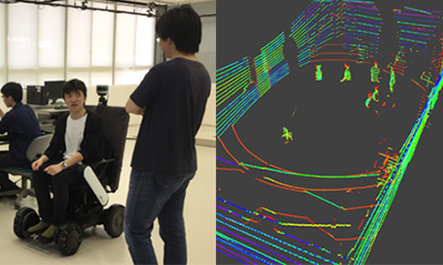
Testing an electric wheelchair equipped with LiDAR.
FUTURE-PV Laboratory
Sputtering system for fabricating solar cells (ITO and SiNx).
Photolithography system for microfabrication of semiconductor devices.