Research Center for Nano-Electronics
- KEYWORDS
- Semiconductor materials
- Optoelectronic devices
- ●High-performance and low-power-consumption electronic devices
- ●Highly efficient light emitting devices for optical interconnections
- ●Group-IV semiconductor epitaxial growth and lattice strain control
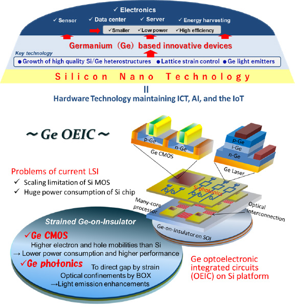
Today’s highly advanced information communication technology (ICT) is based on semiconductor nanoelectronics, but difficulties in achieving further performance improvements and their huge power consumption levels are critical issues worldwide. To overcome these problems, we are developing next-generation low-power-consumption optoelectronic devices, such as, high-mobility transistors and light-emitting devices that utilize strained germanium (Ge) thin films and Ge quantum nanodots, by employing the crystal growth and semiconductor process equipment installed in our clean room.
Research staff
Head・Professor
Si/Ge crystal growth, Heterostructure devices
Professor
Control of MIS interfaces, Evaluation of interface properties
Professor
Nano device reliability engineering
Associate Professor
Two dimensional (2D) materials, Evaluation of optical properties
Professor
Electronic & Electric materials, Energy-related chemistry

Associate Professor
Crystal growth, Semiconductor spintronics
Professor / The University of Tokyo Emeritus Professor
Quantum transport, Quantum information, Spintronics
Emeritus Professor
Photonic devices, Simulation
Research Assistant Professor
Mahfuz Alam
Semiconductor engineering

Research themes
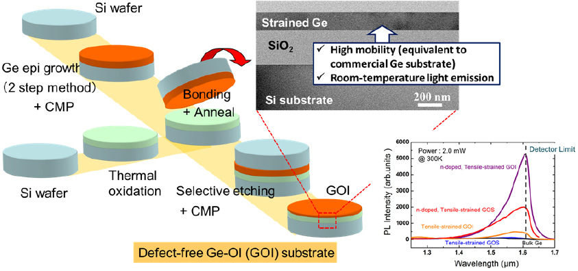
Strained Ge-on-Insulator
To create high-performance Ge-based electronic and optical devices, high -quality Ge thin layers possessing the crystal strain have to be formed on Si wafers. To accomplish this, we have developed Ge epitaxy and wafer transfer techniques that allow us to realize high quality strained Ge-on-Insulators on Si wafers.
Strained Ge channel devices
have been obtained from strained Ge channel structures. Moreover, by using our atomic layer deposition (ALD) system, which is connected to the MBE chamber, we can form high-quality interfaces between gate insulators and Ge channels, and thus realize ultra high-mobility Ge channel MOSFETs.

Ge Photonic devices
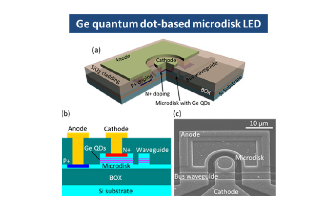
To create semiconductor chips with ultra-low power consumption levels, optical interconnections on silicon chips are extremely important and light sources that are monolithically integrated on Si are necessary. To this end, we are researching strained-Ge and Ge quantum dot-based light emitters that can be epitaxially grown on Si. Such emitters, when combined with microcavities, such as microdisks and photonic crystals, will help us to realize highly efficient Si-based light emitters and optical interconnections.
Ge microdevices
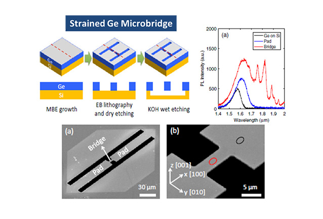
Band engineering based on lattice strain introduction can alter structures from indirect to direct band types, thereby opening routes to the use of various applications on Si-based optical devices. Previously, we have succeeded in introducing very large lattice strains into Si/Ge based microstructures, such as Microbridges, which are fabricated by selective etching of Ge-on-Si and GOI wafers. In the future, we aim to develop novel devices with new functions by combining micro-resonant structures with MEMS devices.
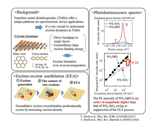
Novel atomic layer material based devices
We study their fundamental optical properties of transition metal dichalcogenides (TMDs) and clarify their unknown material properties in order to propose and develop novel next-generation devices.